ODrive Pro Datasheet
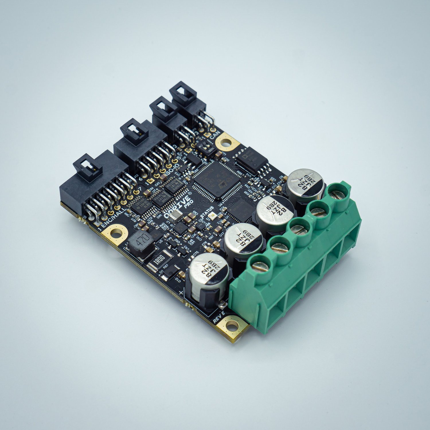
The ODrive Pro is the high-performance flagship of ODrive Robotics’s motion control lineup, bringing 5kW peak power and robust isolated interfaces to power any demanding and rigorous robotics application.
Electromechanical Specifications
Electrical
Note
All specifications are in 0◦C ≤ TA≤ 40◦C unless otherwise noted.
Specification |
Min. |
Typ. |
Max. |
Units |
Conditions and Notes |
|---|---|---|---|---|---|
DC Voltage |
15 |
58 |
V |
||
Maximum Modulation Depth |
99% |
Utilizable percentage of DC bus voltage |
|||
AUX Logic Voltage |
10 |
12 |
14 |
V |
Optional |
Operating Motor Current |
20 80 100 |
A A A |
Free air (TA 25°C) Active cooling (TA25°C) Peak (3 second max) |
||
ESD Protection |
±30 ±8 ±8 ±8 ±8 ±6 |
kV |
Power Lines, IEC 61000-4-2 CAN Lines, IEC 61000-4-2 Isolated Lines, IEC 61000-4-2 RS485 Lines, IEC 61000-4-2 USB Lines, IEC 61000-4-2 All Other Lines, IEC 61000-4-2 |
||
CAN baudrate |
12 |
Mbit/s |
Additional firmware limitations apply, see |
Physical
Specification |
Value |
Units |
Notes |
|---|---|---|---|
Mass |
140 72 32 |
g |
Full Case Heat Spreader Bare Board |
Width Length Height |
51 64 17.5 |
mm |
|
Mounting |
PCB Heat Spreader |
4x M3, 42mm x 45mm pattern (horizontal, vertical) 4x M4, 60mm x 60mm pattern |
|
Connectors
Connector mating receptacles and crimps.
Connector |
Description |
Connector P/N |
Mating Receptacle |
Mating Crimp |
Precrimped Wire P/N |
|---|---|---|---|---|---|
Power |
Optional Screw Terminal |
TB005-762-05BE |
N/A |
N/A |
N/A |
J8 |
Motor/Encoder Feedback |
1053141214 |
1053081214 |
1053001200 |
0797582129 |
J12 |
Isolated Signals |
1053141210 |
1053081210 |
1053001200 |
0797582129 |
J13, J9 |
CAN Header |
1053141204 |
1053081204 |
1053001200 |
0797582129 |
J14 |
Additional Feedback |
SM12B-GHS-TB |
GHR-12V-S |
SSHL-002T-P0.2 |
AGHGH28K305 |
J7 |
Debug Header |
SM05B-GHS-TB |
GHR-05V-S |
SSHL-002T-P0.2 |
AGHGH28K305 |
Environmental
Specification |
Value |
Notes |
|---|---|---|
Humidity |
Non-Condensing |
|
Ingress Protection |
IP20 |
with case |
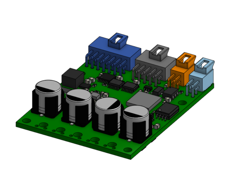
CAD
The CAD models for the ODrive Pro and all of its accessories are available on our OnShape page.
Pinout
Power Pads
Important
DC+- cannot tolerate reversed polarity, verify all power pad connections before energizing.
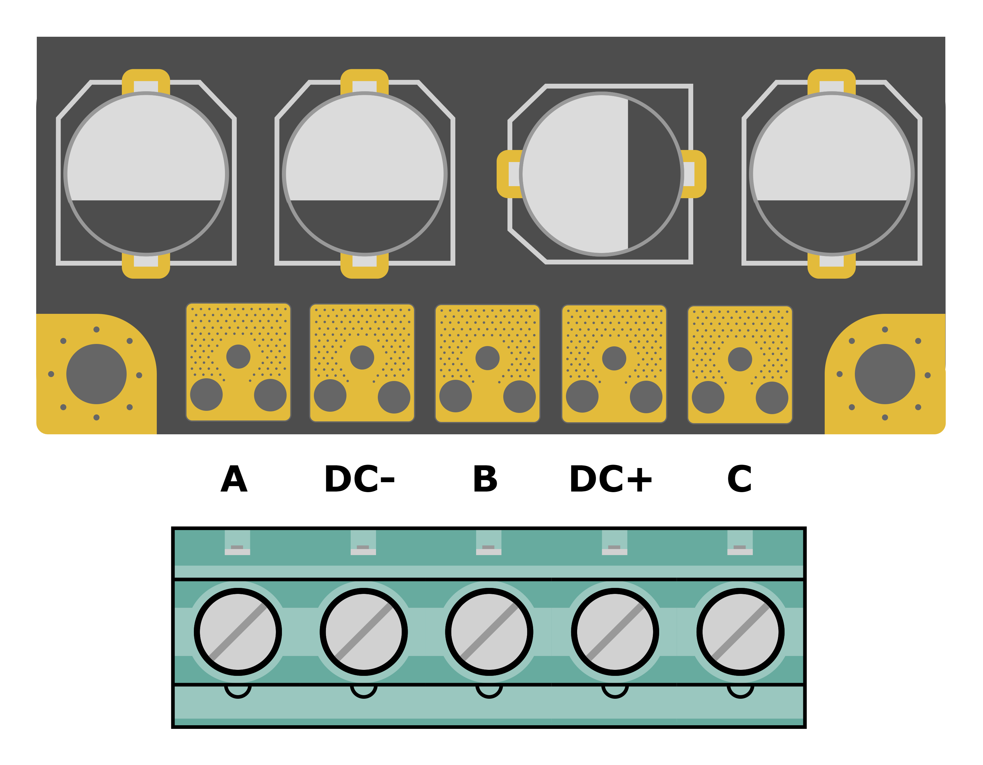
Pin |
Description |
|---|---|
A |
Motor phase A |
DC- |
Power ground |
B |
Motor phase B |
DC+ |
Power input, referenced to DC- |
C |
Motor phase C |
The motor phase connections A/B/C can be connected in any order.
Logic Pins
Digital mode is a general purpose mode that can be used for these functions: step, dir, enable, encoder index, hall effect encoder, SPI encoder nCS.
All GPIO pins are 5V tolerant, except if you power the isolator with 3.3V, then ISOLATED IO inputs are rated to 3.3V nominal.
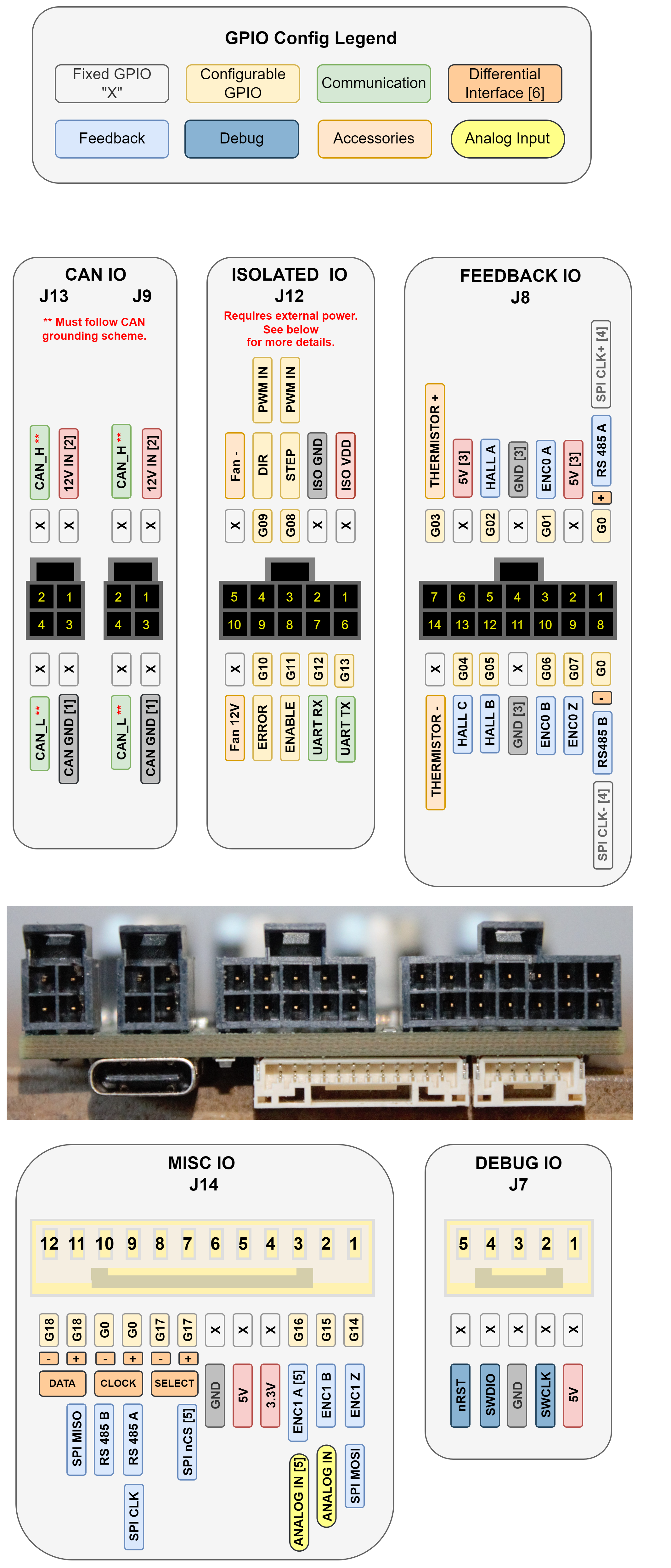
GPIO Properties
Additional notes and properties for each GPIO pin
Note
The letter G and the zero padding are not used in odrivetool or the web GUI, i.e. G09 would be represented by only the number 9.
G0: This pin is driven at RS422 logic levels, and cannot be used as a logic input. This pin cannot be used if an external SPI encoder is used. The + and - pins are complementary outputs.
G01-G07: The HALL and ENC0 pins have a 2.7kΩ pullup to +5V, and HALL pins have a low pass filter (τ=4.25us). These pins are on the output of a digital isolator, and cannot be used in output mode. When used as an input, they cannot be used in DIGITAL_PULL_DOWN mode.
G03: The THERMISTOR+ pin has an internal 1kΩ pullup to 3.3V for use in a thermistor sense circuit. It cannot be used in DIGITAL_PULL_DOWN mode.
G08, G09, G11, G12: See ISOLATED IO section for required information using isolated pins. These pins are connected to a digital isolator, and can be used as GPIO inputs only. There is a 1.5MΩ pull-down integrated to the isolator, and pull up/down configuration has no effect.
G10, G13: See ISOLATED IO section for required information using isolated pins. This pins is connected to a digital isolator, and can be used as a GPIO output only.
G14-G16: The ENC1 A/B/Z pins are connected to the ODrive Pro through a 1kΩ series resistor. When using these pins in output mode, drive strength will be reduced.
G17: This pin is driven at RS422 logic levels, and cannot be used as a logic input. The + and - pins are complementary outputs.
G18: This pin is recieved at RS422 logic levels, and cannot be used as a logic output. The + and - pins are complementary inputs. If using a single-ended SPI transciever, leave the - pin floating.
User Facing Pins (Gxx)
Locations for all pins that can be configured using
GpioMode.- Inputs:
G0-G02, G04-G09, G11-G12, G14-G16, G18
- Outputs:
G0, G03, G10, G13-G17
Note
Inputs and outputs are not mutually exclusive.
Notes
5V outputs: combined draw max 600mA
The 5V output has an output voltage range across load of 4.6-4.9V. For reliability, ensure your encoder has a minimum input voltage rating of 4.5V or below.
CAN IO
[1] CAN_GND must be connected to DC- at a single point (system star point) when using the CAN interface. See system grounding scheme for more details.
[2] CAN_12V is optional and is used to power the ODrive logic, enabling communication before the main power supply is connected. Allowed voltage range: 10V-14V
FEEDBACK IO
[3] GND and 5V+ are filtered (ferrite/capacitor) from DC-.
THERMISTOR + has an integrated 1k ohm voltage divider.
Maximum frequency of A/B inputs of ENC0 and ENC1 is software-configurable:
<inc_encoder>.config.filter
Warning
[4] The differential signal pin(s) GO+, G0- are located on J8 AND J14
ISOLATED IO
ISO_GND and ISO_VDD must be connected to your other board.
ISO_VDD is a power Input to the isolated interface, which you should power with 3.3V or 5V.
Input and output levels are 3.3V if you supply 3.3V, and are 5V if you supply 5V. Inputs are not 5V tolerant if you supply 3.3V.
Power Output Instead of Input (requires hardware modification)
You can change the ISO VDD and ISO GND to be power outputs instead, but this will bypass the isolation. This can be useful if you are powering a module that doesn’t have any other connections than to the ODrive, such as an RC receiver. To do this, you can bridge R66 and R64 for 5V output, or R66 and R65 for 3.3V output, on ISO VDD.
MISC IO
3.3V max draw 200mA
see Differential Interfaces below.
Warning
[5] Pins G14, G15, and G16 are only rated for 3.3v, they are NOT 5V tolerant.
Differential Interfaces [6]
Pins G0 [clock], G17 [select] and G18 [data] can be used for RS422 differential signals or as single ended connections if only the + side is used. This allows the ODrive Pro to support a wide variety of encoder interfaces, including SSI (RS422 or single ended), BiSS or RS422 SPI (half duplex only). For specific encoder protocols please refer to the Encoders Page.