ODrive S1 Datasheet
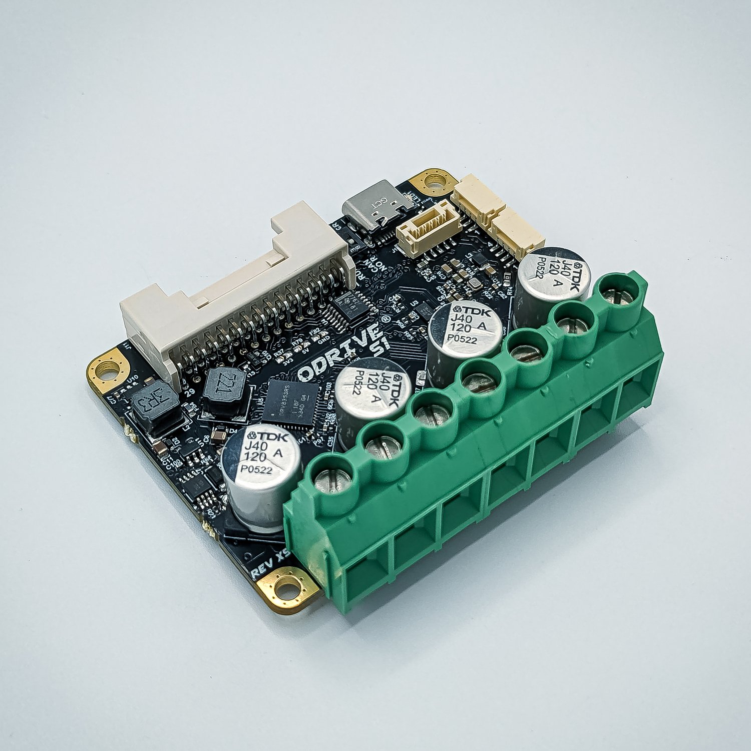
The ODrive S1 brings ODrive’s next-generation motion control ecosystem to every robot, with a 2kW continuous power output and a wide variety of encoder interfaces, all at an accessable price point and with a form factor smaller than a credit card.
Electromechanical Specifications
Electrical
Note
All specifications are in 0◦C ≤ TA≤ 40◦C unless otherwise noted.
Specification |
Min. |
Typ. |
Max. |
Units |
Conditions and Notes |
|---|---|---|---|---|---|
DC Voltage |
12 |
16-48 |
50.5 |
V |
|
Maximum Modulation Depth |
78% |
Utilizable percentage of DC bus voltage |
|||
AUX Logic Voltage |
10 |
12 |
14 |
V |
Optional |
Operating Motor Current |
20 40 40-80 |
A A A |
Free air (TA 25°C) Heat spreader plate (TA 25°C) Peak, see below |
||
ESD Protection |
±30 ±13 ±8 ±8 ±6 |
kV |
Power Lines, IEC 61000-4-2 CAN Lines, IEC 61000-4-2 Isolated Lines, IEC 61000-4-2 USB Lines, IEC 61000-4-2 All Other Lines, IEC 61000-4-2 |
||
CAN baudrate |
8 |
Mbit/s |
Additional firmware limitations apply, see |
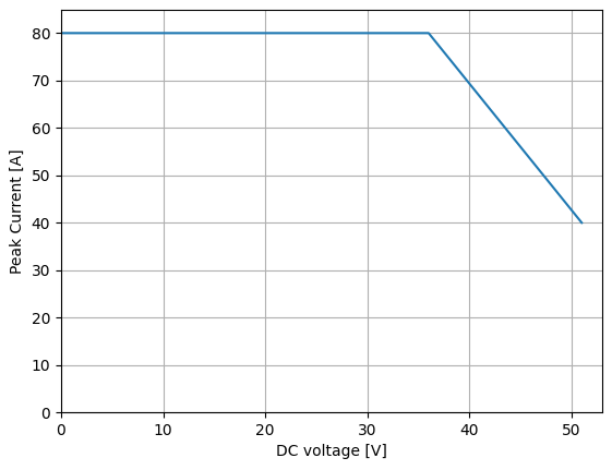
ODrive S1 Peak Current vs DC voltage.
The firmware limits motor current according to this curve depending on dc_bus_overvoltage_trip_level.
Connectors
Connector mating receptacles and crimps.
Connector |
Description |
Connector P/N |
Mating Receptacle |
Mating Crimp |
Precrimped Wire P/N |
|---|---|---|---|---|---|
Power |
Optional Screw Terminal |
TB005-762-07BE |
N/A |
N/A |
N/A |
J11 |
Unified I/O Header |
S30B-PUDSS-1 |
PUDP-30V-S |
SPUD-002T-P0.5 |
ASPUDSPUD22K305 |
J16, J17 |
CAN Header |
SM04B-GHS-TB |
GHR-04V-S |
SSHL-002T-P0.2 |
AGHGH28K305 |
J1 |
Debug Header |
BM05B-GHS-TB |
GHR-05V-S |
SSHL-002T-P0.2 |
AGHGH28K305 |
Environmental
Specification |
Value |
Notes |
|---|---|---|
Humidity |
Non-Condensing |
|
Ingress Protection |
IP20 |
with case |
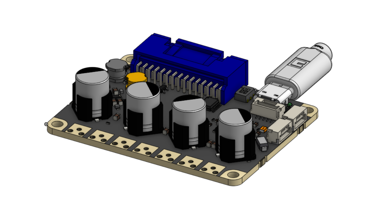
CAD
The ODrive S1 CAD model is available on the ODrive S1 OnShape page.
Pinout
Power Pads
Important
DC+- cannot tolerate reversed polarity, verify all power pad connections before energizing.
Important
Do not connect multiple S1s to a single brake resistor! Each S1 must utilize its own separate brake resistor.
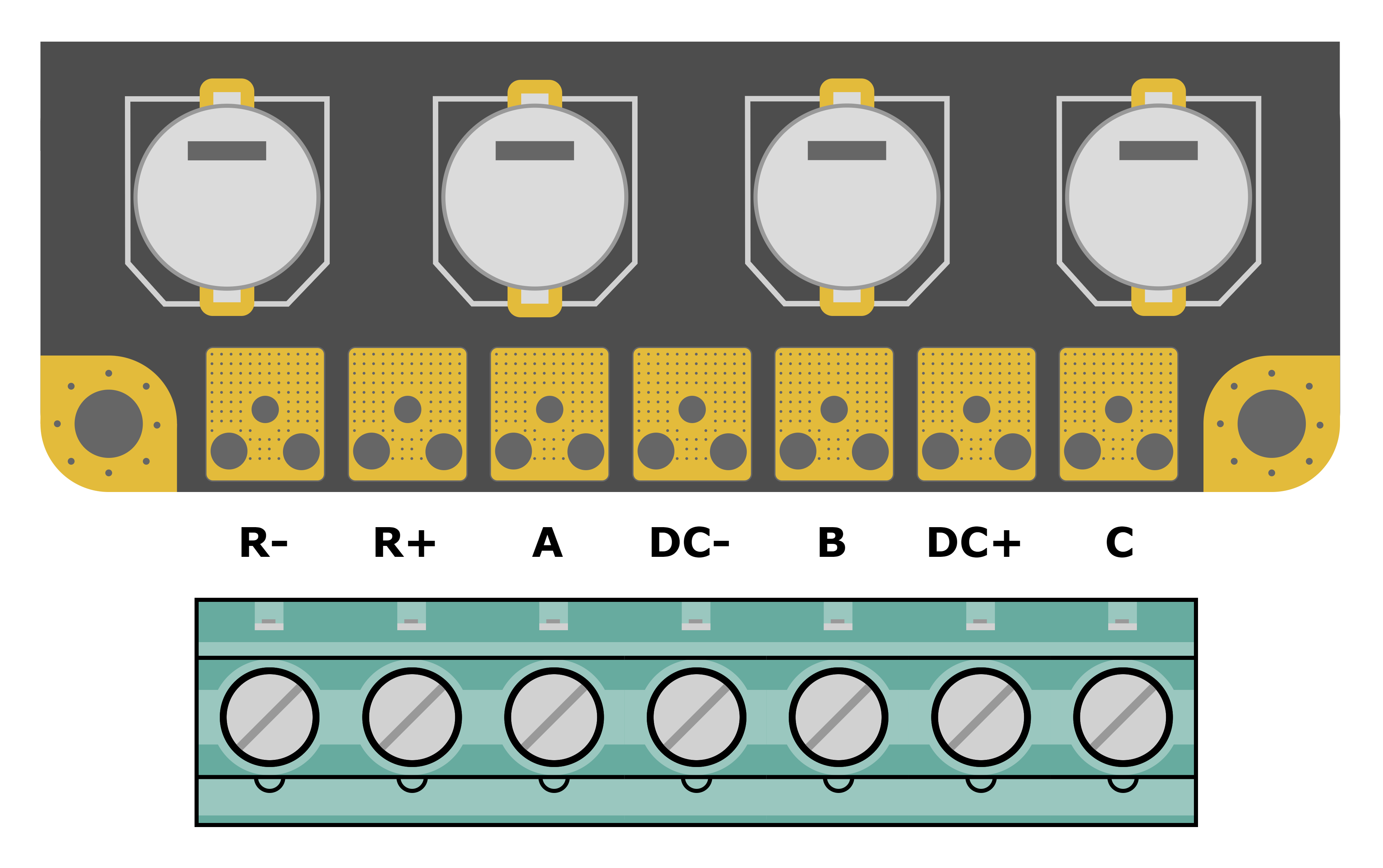
Pin |
Description |
|---|---|
R- |
Brake resistor output |
R+ |
Brake resistor output |
A |
Motor phase A |
DC- |
Power ground |
B |
Motor phase B |
DC+ |
Power input, referenced to DC- |
C |
Motor phase C |
The motor phase connections A/B/C can be connected in any order.
Logic Pins
Digital mode is a general purpose mode that can be used for these functions: step, dir, enable, encoder index, hall effect encoder, SPI encoder nCS.
All GPIO pins are 5V tolerant, except if you power the isolator with 3.3V, then ISOLATED IO inputs are rated to 3.3V nominal.
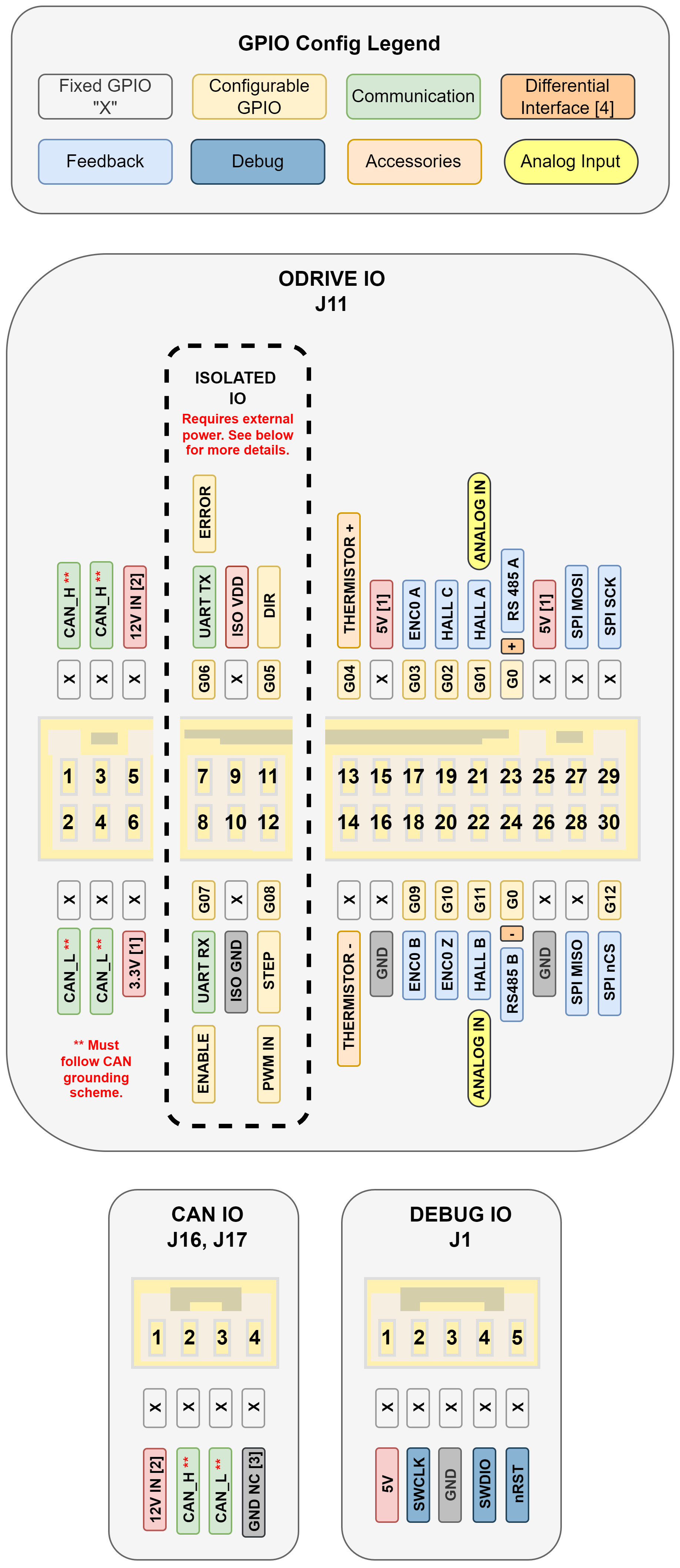
GPIO Properties
Additional notes and properties for each GPIO pin
Note
The letter G and the zero padding are not used in odrivetool or the web GUI, i.e. G09 would be represented by only the number 9.
G0: This pin is driven at RS422 logic levels, and cannot be used as a logic input. This pin cannot be used if an external SPI encoder is used. The + and - pins are complementary outputs.
G01, G02, G11: The HALL pins have a 2.7kΩ pullup to +5V and low pass filter (τ=4.25us), and cannot be used in DIGITAL_PULL_DOWN mode. When used as an output, the logic low level will be 500mV.
G03, G09, G10: The ENC0 pins have a 2.7kΩ pullup to +5V, and cannot be used in DIGITAL_PULL_DOWN mode. When used as an output, the logic low level will be 500mV.
G04: The THERMISTOR+ pin has an internal 1kΩ pullup to 3.3V for use in a thermistor sense circuit. It cannot be used in DIGITAL_PULL_DOWN mode.
G12: This pin can only be used as a SPI nCS pin, and should not be configured as a user-controlled input or output.
G05, G07, G08: See ISOLATED IO section for required information using isolated pins. These pins are connected to a digital isolator, and can be used as GPIO inputs only. There is a 1.5MΩ pull-down integrated to the isolator, and pull up/down configuration has no effect.
G06: See ISOLATED IO section for required information using isolated pins. This pins is connected to a digital isolator, and can be used as a GPIO output only.
User Facing Pins (Gxx)
Locations for all pins that can be configured using
GpioMode.- Inputs:
G0-G03, G05, G07-G11
- Outputs:
G0-G03, G06, G09-G11
Note
Inputs and outputs are not mutually exclusive.
Notes
5V outputs: combined draw max 150mA
3.3V output: max draw 150mA
[1] 5V and 3.3V can be switched on and off internally. (feature coming soon!)
The RS485 and SPI feedback interfaces are mutually exclusive on S1 – a RS485 and external SPI encoder cannot be used at the same time
THERMISTOR + has an integrated 1k ohm voltage divider.
[2] 12V in is optional and is used to power the ODrive logic, enabling communication before the main power supply is connected. Allowed voltage range: 10V-14V. Referenced to DC-. This voltage range is a hard limit, and inrush and overvoltage protection must be guaranteed.
[3] GND NC offers a common connection for the CAN bus ground; it is not connected internally.
[4] Differential interface used for RS-485 encoders.
ISOLATED IO (G05-G08)
GND ISO and V+ ISO must be connected to your other board.
V+ ISO is a power Input to the isolated interface, which you should power with 3.3V or 5V.
Input and output levels are 3.3V if you supply 3.3V, and are 5V if you supply 5V. Inputs are not 5V tolerant if you supply 3.3V.
UART: (TX)-Transmit data from ODrive, (RX)-Recieve data to ODrive.
The isolated inputs don’t have a built-in pull-up/pull-down resistor (neither user configurable nor fixed). Setting the GPIO mode to
DIGITAL_PULL_UPorDIGITAL_PULL_DOWNon these pins has the same effect asDIGITAL.